Current project downloads
Current R15 assembly, routing, schematic and editable KiCad files, alongside preserved earlier CAD and FPGA reviews.
Current XEM8305 / LDO carrier R15 · 12 October 2026
Six-layer, 53 × 83 mm routed review candidate with 437 widened power/ground sections. Editable native project includes local public-safe models; electrical and routing geometry is preserved. The full XEM–carrier–LDO illustration shows MC1–MC3 and J1/J19, with nominal 5 mm and 2 mm mating gaps. Qualification remains open.
Open full assembly and routing · Complete KiCad ZIP · R14 → R15 comparison PDF · One-page schematic · Checks
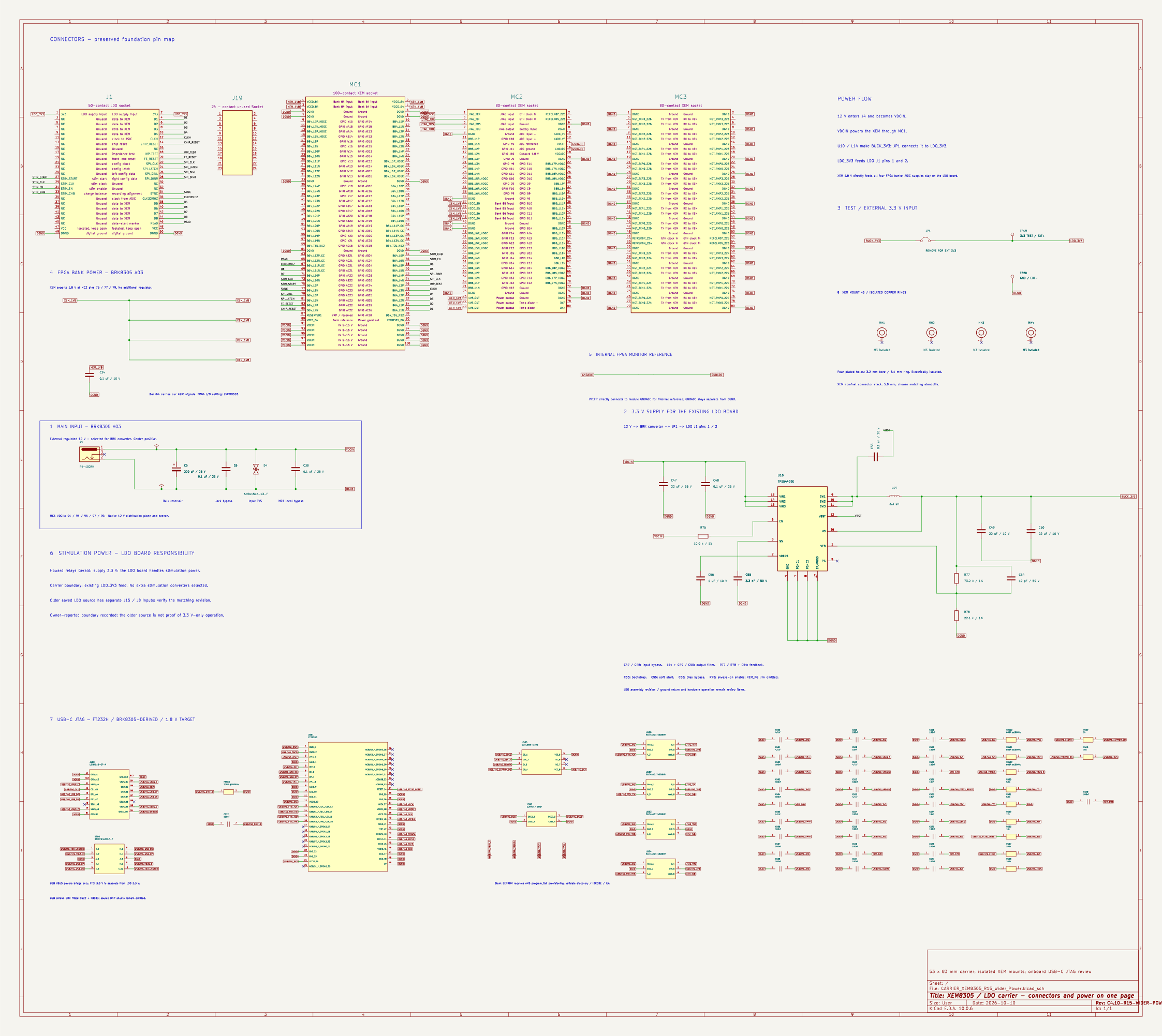
Earlier R5 Gerbers do not match R15. This delivery is a design review, not a fabrication release.
Earlier XEM8305 / LDO carrier · R12
9 October 2026 · six copper layers · 53 × 83 mm · 75 fitted component bodies. D4 is moved outside the aligned LDO outline, with 2.50 mm nominal side clearance. The current review includes six selectable routing layers, draggable/zoomable copper views, rotatable component 3D and BRK8305-derived USB-C JTAG.
Open interactive routing and 3D · R12 one-page schematic · R12 checks and qualification · Visual sources and hashes · LDO mating-space comparison
These are CAD-rendered review images. Some connector bodies use simplified package representations. R12 native PCB checks report zero violations, opens and parity findings under retained settings; inherited schematic ERC findings and hardware qualification remain open. The JTAG EEPROM still needs programming. Not a fabrication release.
The R5 CAD and four-layer Gerbers below are an earlier delivery and do not match this six-layer R12 board.
Earlier XEM8305 / LDO carrier · R11
9 October 2026 · six copper layers · 53 × 83 mm · 75 fitted component bodies. This preserved review includes six selectable routing layers, draggable/zoomable copper views, rotatable component 3D and BRK8305-derived USB-C JTAG.
Open interactive routing and 3D · R11 one-page schematic · R11 checks and qualification · Visual sources and hashes
These are CAD-rendered review images. Some connector bodies use simplified package representations. R11 native PCB checks report zero violations, opens and parity findings under retained settings; inherited schematic ERC findings and hardware qualification remain open. The JTAG EEPROM still needs programming. Not a fabrication release.
The R5 CAD and four-layer Gerbers below are an earlier delivery and do not match this six-layer R11 board.
Earlier carrier files · C4.8-R5
9 October 2026 · four copper layers · 53 × 83 mm · KiCad 10. TP21 is removed. TP19/TP20, the aligned corner vias and connector positions are retained.
Download editable KiCad project · Download matching Gerbers and drills · View the one-page schematic
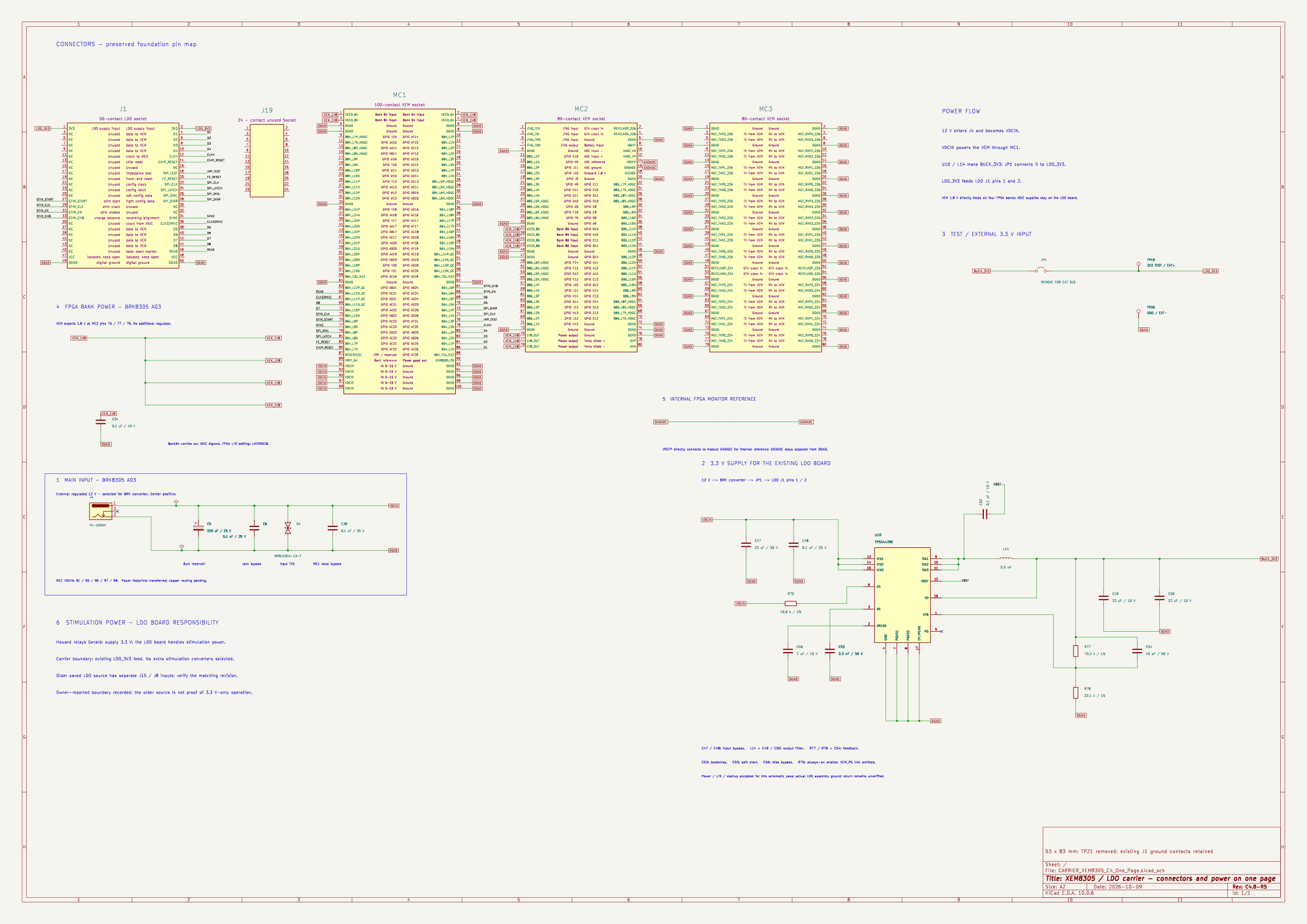
Extract the entire KiCad ZIP and open project/CARRIER_XEM8305_C4_One_Page.kicad_pro. Schematics, board, rules and local symbol/footprint libraries are included. J1 is the 50-pin Hirose DF40C(2.0) socket; J19 is its 24-pin counterpart. Restricted Hirose and Samtec 3D bodies are omitted, with exact optional-model paths and manufacturer links documented inside the package. The complete models remain in the local working project.
Where each power rail goes
| Rail | Connection | Purpose |
|---|---|---|
| 12 V | Barrel input → XEM MC1 VDCIN | Main power for the XEM8305 |
| 3.3 V | Carrier converter → JP1 → LDO J1 pins 1/2 | Power input to the LDO/ASIC assembly |
| 1.8 V | XEM module output → FPGA VCCO pins | FPGA I/O-bank supply |
The XEM's main input receives 12 V. The separate 3.3 V converter feeds the LDO/ASIC assembly. Opal Kelly specifies a 5–15 V XEM input and recommends 12 V; official power documentation also explains the module-provided 1.8 V bank supply.
Revision and check details · Download checksums
Fresh public-package PCB checks report zero violations, unconnected items and schematic/PCB parity findings. Inherited schematic ERC findings and electrical, mechanical and factory qualification remain open. Review files; not a fabrication release.
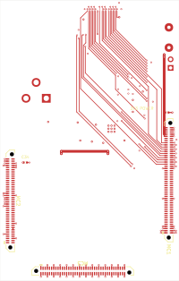
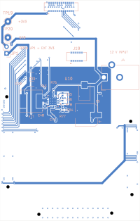
Inspect the preserved R5 top and bottom routing
Preserved carrier · C4.8-R4
Published 9 October 2026 · four copper layers · 53 × 83 mm · KiCad 10. This preserved routing review retains the original outline and aligns the corner signal vias.
Download editable KiCad project · Download Gerber and drill ZIP
Extract the entire KiCad ZIP before opening project/CARRIER_XEM8305_C4_One_Page.kicad_pro. The public package includes the schematic, board, rules and local libraries. Two embedded Samtec STEP models are omitted, with external model dependencies documented. The complete local handoff is preserved.
Revision, checks and package details · Download checksums
The saved R4 board has zero reported DRC violations, open connections and schematic/PCB parity findings. Inherited schematic ERC findings still require cleanup; power, timing, mechanical and factory qualification remain open. These are review files, not a fabrication release.
View the routing and corner alignment
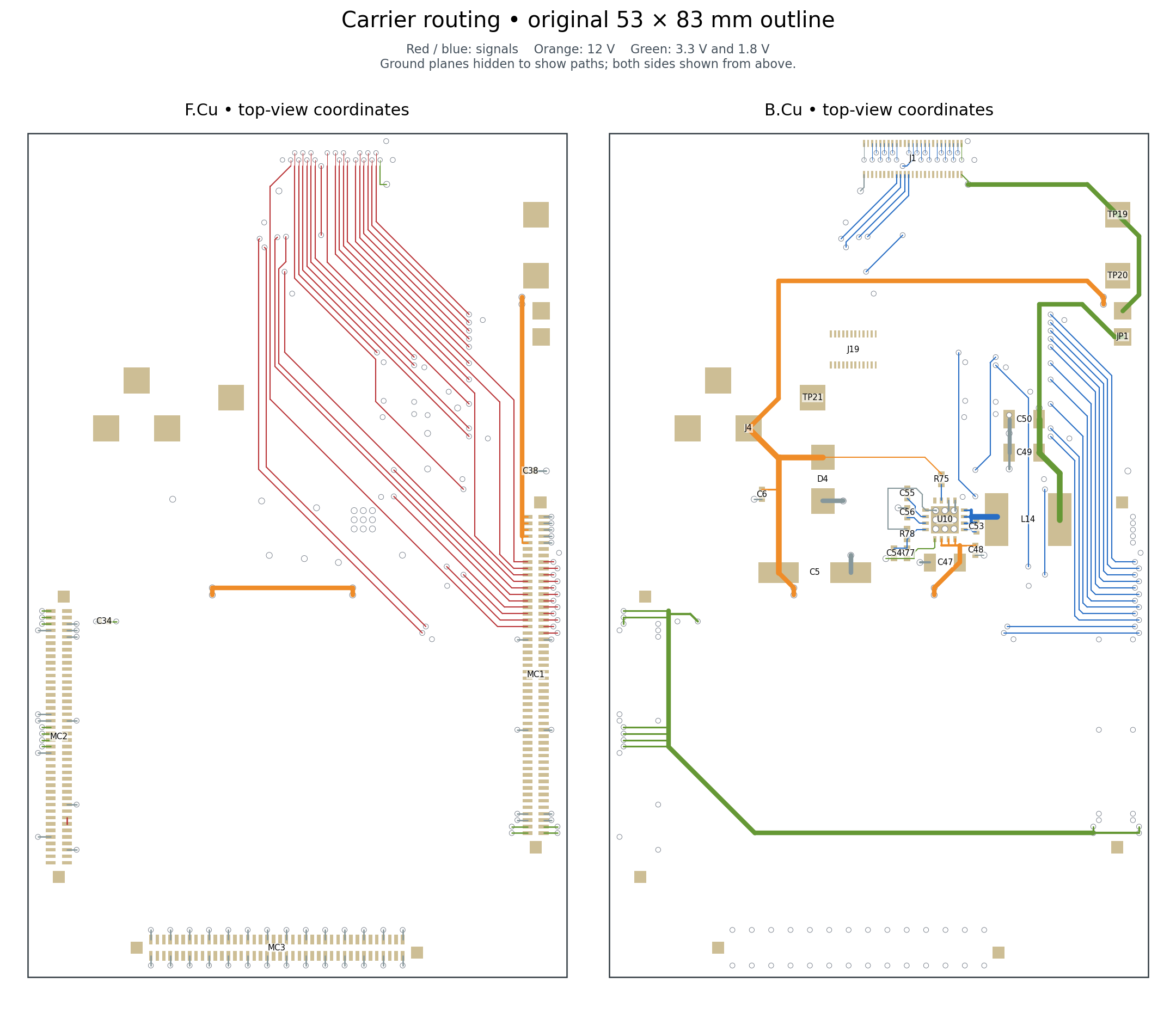
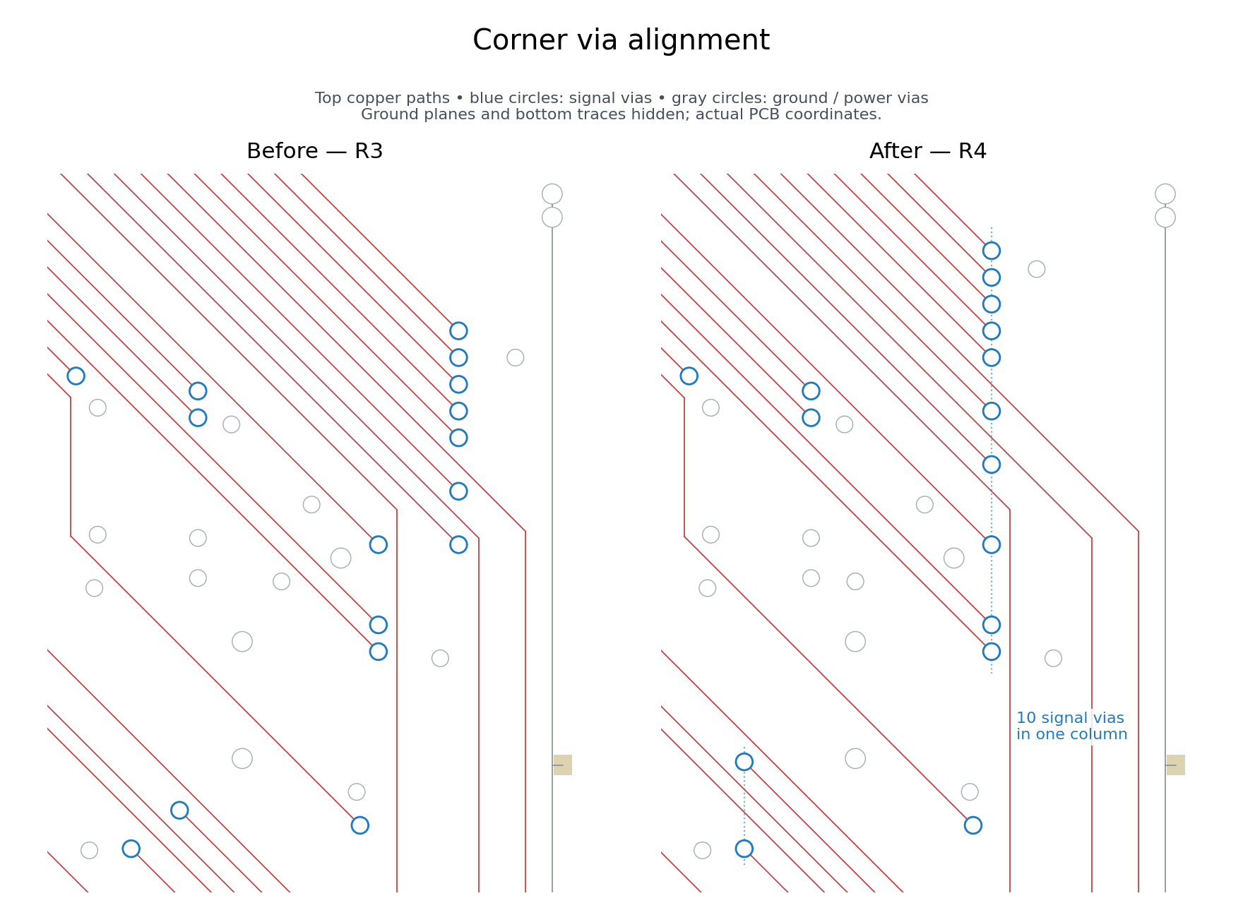
Preserved 5 October direct-carrier R3 review and files remain a separate earlier design.
Custom FPGA · 35T R39
5 October 2026 · 41 × 41 mm · KiCad 10.0.6 · all 18 schematic sheets, project rules, local libraries and 34 model files. Extract the whole ZIP before opening hardware/FPGA35T_V15.kicad_pro.
Download complete R39 KiCad project (2.86 MiB)
Native check summary and project status · Board views and progress
Research revision; not for fabrication. Routing remains incomplete. The factory construction, critical routing and hardware qualification still need completion.
SHA-256 checksum
a020c3d0848a9ae5bb0c65421e31aa7087639a2a6a19dac82dc85663ea4052c3Preserved direct LDO + XEM8305 · R2
5 October 2026 · all MC1/MC2/MC3 contacts accounted for · both J1/J19 LDO mating connectors · four complete schematic sheets and local libraries. Extract the whole ZIP before opening hardware/LDO_to_XEM8305_Direct_R2.kicad_pro. Two embedded Samtec model payloads are omitted and their external references documented; non-model native semantics are preserved.
Download native R2 KiCad project (288.4 KiB) · Complete schematic · 4-page PDF (255.3 KiB)
Checks and qualification limits · 260-contact CSV · Preserved R2 top/bottom and rotatable carrier review
Routed CAD candidate. Fresh extracted-project ERC / DRC / opens / parity are zero. MC3 has 28 DGND contacts and 52 explicitly reserved no-connects. Exact assembled fit, ASIC timing, power/load/thermal, FPGA firmware, factory DFM and operation remain unqualified.
Native ZIP SHA-256
eff6401e7ca90485d8b24f7f87177de92050b947d1d3863b339121e50a191b91Schematic PDF SHA-256
ad3e3e43612bde56d2d48368ed6193ce76f9795f93367868faecab73f4fdd160The earlier R37 review and other dated studies remain in the Library.