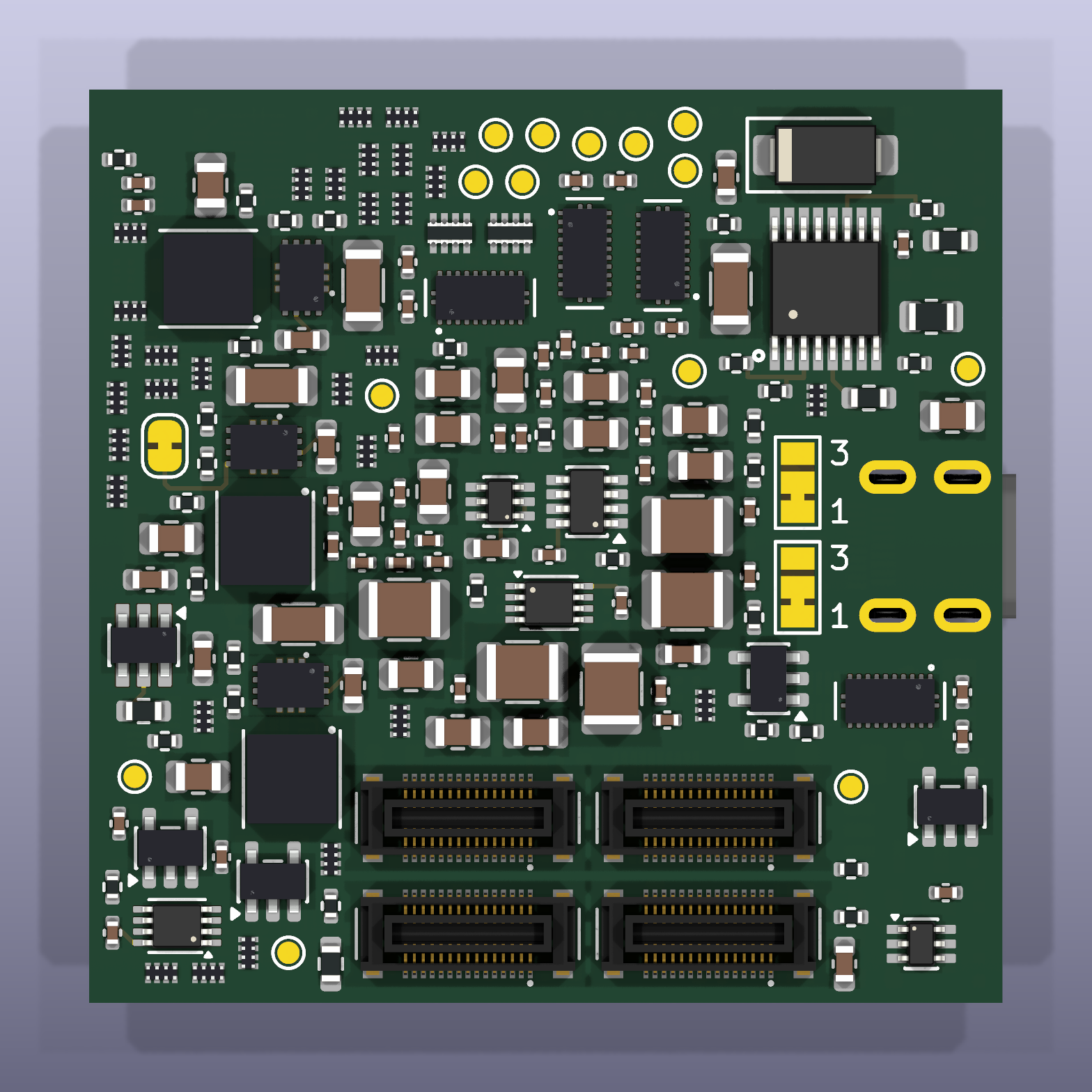
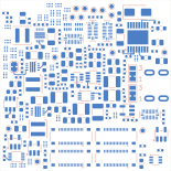
The 41 × 41 mm XC7A35T-2CSG325I board now has corrected land patterns and silkscreen, bounded FPGA escape rules and updated component information. The four floating Hirose connectors remain grouped on the underside.
R39 · research revision343 components41 × 41 mm PCB18 schematic sheets
Saved R39 native board
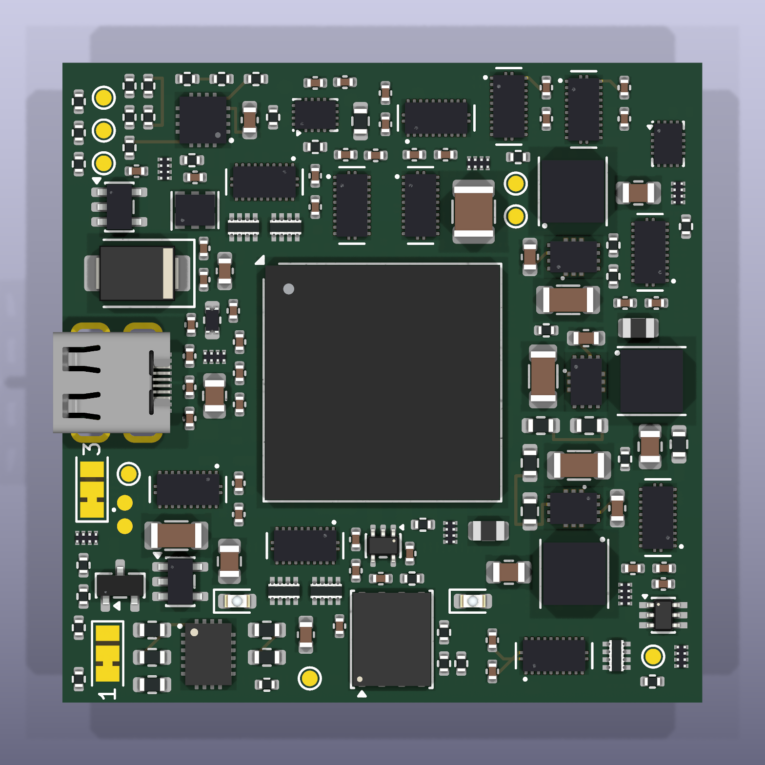
Top and bottom views
Top. FPGA in the center, with the existing surrounding power and interface circuitry. Full-size image.Bottom. Four Hirose connectors grouped together, viewed directly from underneath. Full-size image.
Fresh KiCad renders from R39. Component models depict nominal geometry; routing and populated fit remain incomplete. The 1.6 mm CAD thickness is an inherited placeholder.
Rotatable R39 headboard
Open the 3D view to rotate the board.
Drag to rotate · scroll to zoom · right-drag to pan
Current headboard only, including existing surface copper. The earlier connector-only lower-board template is retained in the dated R37 review.
Applied changes
What changed in R39
Land patterns and silkscreen
Retains 323 supplier-supported land corrections and improved silkscreen. The remaining fine-pitch TI/Hirose lands keep their accurate supplier geometry; JLCPCB’s exact-part library corroborates these narrow-land families.
FPGA routing rules
Fine escape rules are confined to the FPGA area. Ordinary spacing and unrelated bottom-side pads retain their existing protections. The adjacent laser-via candidate uses 0.35 mm lands and 0.125 mm drills.
Component information
Corrects 31 engineering and purchasing fields on 11 components, including actual regulator nominal voltages and the manufacturer’s current alias for six capacitors.
Native checks
Physical DRC, ERC and schematic/PCB parity pass under the delivered project settings. All existing placement, pad assignments and 113 surface track segments are preserved.
“Unconnected” means awaiting PCB copper. The schematic net assignments are intact. Native connectivity counts 1,413 PCB connections awaiting copper; the DRC listing is capped at 499. There are no placed vias or completed copper planes.
The eight-layer 3+2+3 HDI construction remains an engineering candidate. JLCPCB must issue the stack, via and impedance/stencil process before critical routing and fabrication. One consolidated request is prepared and unsent. Passing CAD checks does not establish fabrication or powered-operation readiness.
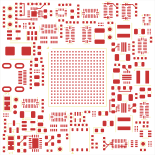
These views show saved R39 copper, rather than schematic connection lines or future routes.
Editable project
Download R39
Extract the whole ZIP and open hardware/FPGA35T_V15.kicad_pro in KiCad 10.0.6. The project includes all 18 schematic sheets, rules, local libraries and 34 component-model files. This is a research revision, not a fabrication release.
R39 is the current compact 35T revision. R37’s headboard/mating-template view, the older paused R35 study and historical 25T placement retain their own status.