Current connection direction · 5 October 2026
Direct LDO → routing board → XEM8305
R2 · routed CAD candidate · hardware qualification open
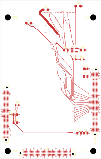
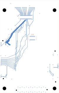
The original LDO board connects through a rigid routing board to XEM8305. This R2 native project includes MC1, MC2 and MC3, both LDO mating connectors, routed intended nets and filled ground copper.
All 260 module contacts accounted for4 schematic sheets · 24 footprints3,508 tracks · 168 vias · 2 zonesFresh public ERC / DRC / opens / parity: 0
Connection scope
Review the complete connector arrangement
MC1, MC2 and MC3
MC1 has 100 contacts; MC2 and MC3 each have 80. Every contact has an audited native pad and schematic disposition. MC3 connects its 28 DGND contacts; the other 52 contacts are explicitly reserved / no-connect. They do not implement a GTH link.
Original LDO board and power
Both J1 and J19 are included for direct mating. J1 carries the mapped ASIC interface and named rails. J19 is preserved as a mechanical mating pair with explicit no-connect contacts. The candidate supplies the module bank rails and keeps the ADC ground reference separate; source, current, sequencing and load qualification remain open.
What still needs qualification
Timing, power and assembled fit
Clock and data routing
The returned clock is 68.476 mm and D_1–D_8 span 69.757–79.765 mm of native copper: an 11.29 mm group spread, with different via counts. These lengths do not establish propagation delay or the provisional ≤100 ps spread. Stack-up, local returns, ASIC setup/hold/data-valid limits and Vivado timing remain open.
Independent power branches
J3 supplies XEM VDCIN; J4 supplies raw VIO 2.5 V ±2%; J5 supplies the original low-stage nominal 3.3 V feed. PG sequences the 1.5 V bank regulator and does not monitor ASIC rails. Actual load, limiting/startup, drop, plating and thermal behavior need qualification.
The carrier includes no automatic powered-off interface isolation, ASIC rail-ready monitor, ASIC hardware current limiter or accepted backfeed/stimulation cutoff. The original high-stage supplies and AGND return still need their accepted source/sequence contract. Firmware high-Z alone does not qualify the power sequence. Exact simultaneous seating, factory DFM and powered recording remain open.
Matching source files
Project, schematic and checks
Extract the whole ZIP and open hardware/LDO_to_XEM8305_Direct_R2.kicad_pro in KiCad 10.0.6. The project contains all four hierarchical sheets, project settings, symbol/footprint tables and local libraries. The two embedded Samtec model files are omitted from this public copy; their external references are documented. Electrical and board geometry semantics match the frozen source.
Fresh checks on the extracted public package report ERC 0, DRC 0, unconnected intended routes 0 and schematic/PCB parity 0. All error, warning and exclusion severities were checked; no checks are ignored or excluded. Full ERC receipt · Full DRC/parity receipt.
The independent assigned-net review passes 790 checks and the actual copper graph review passes 86 checks: all 23 J1→MC1 signals and all 32 multi-pad nets are connected in native copper. Their source bindings and limits are included in the public check summary.
Routed CAD candidate. Simultaneous seating, populated fit, ASIC electrical/timing limits, power/load/thermal behavior, FPGA firmware and factory DFM remain unqualified. These CAD checks do not establish powered recording or fabrication approval. The separate 35T R39 review retains its own status.
Preserved dated reviews
Earlier carrier and adapter studies
The A1R2 assembly and E5 adapter document the earlier cabled topology. Their saved mapping, copper and visualization checks apply to those revisions. The current direct arrangement requires its own native project and checks.