Checked files
Native ERC, DRC, unrouted items and schematic/PCB parity are all zero. The Gerber/drill export passes 144 checks, and actual paste/mask/outline geometry passes 766 checks. No CAD checks are ignored or excluded.
Current carrier · R12 · 9 October: Open the current six-layer carrier and complete component 3D views. The page below is a preserved earlier revision.
Direct LDO → carrier → XEM8305
The existing LDO plugs into this carrier, which plugs directly into XEM8305. One design includes all three XEM sockets, onboard 2.5 V / 3.3 V supplies from an external 12 V input, and the switched ASIC interface.
File sizes and checksums · Checks and remaining qualifications
Open the 3D view to rotate the carrier.
Drag to rotate · scroll to zoom · right-drag to pan
Actual native carrier board, pads and outer copper, with project-authored nominal component envelopes. The envelopes show position and side; exact manufacturer housings and the assembled XEM/LDO stack are omitted. This view does not qualify physical fit. Geometry receipt · Download 3D model.
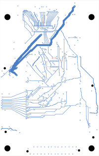
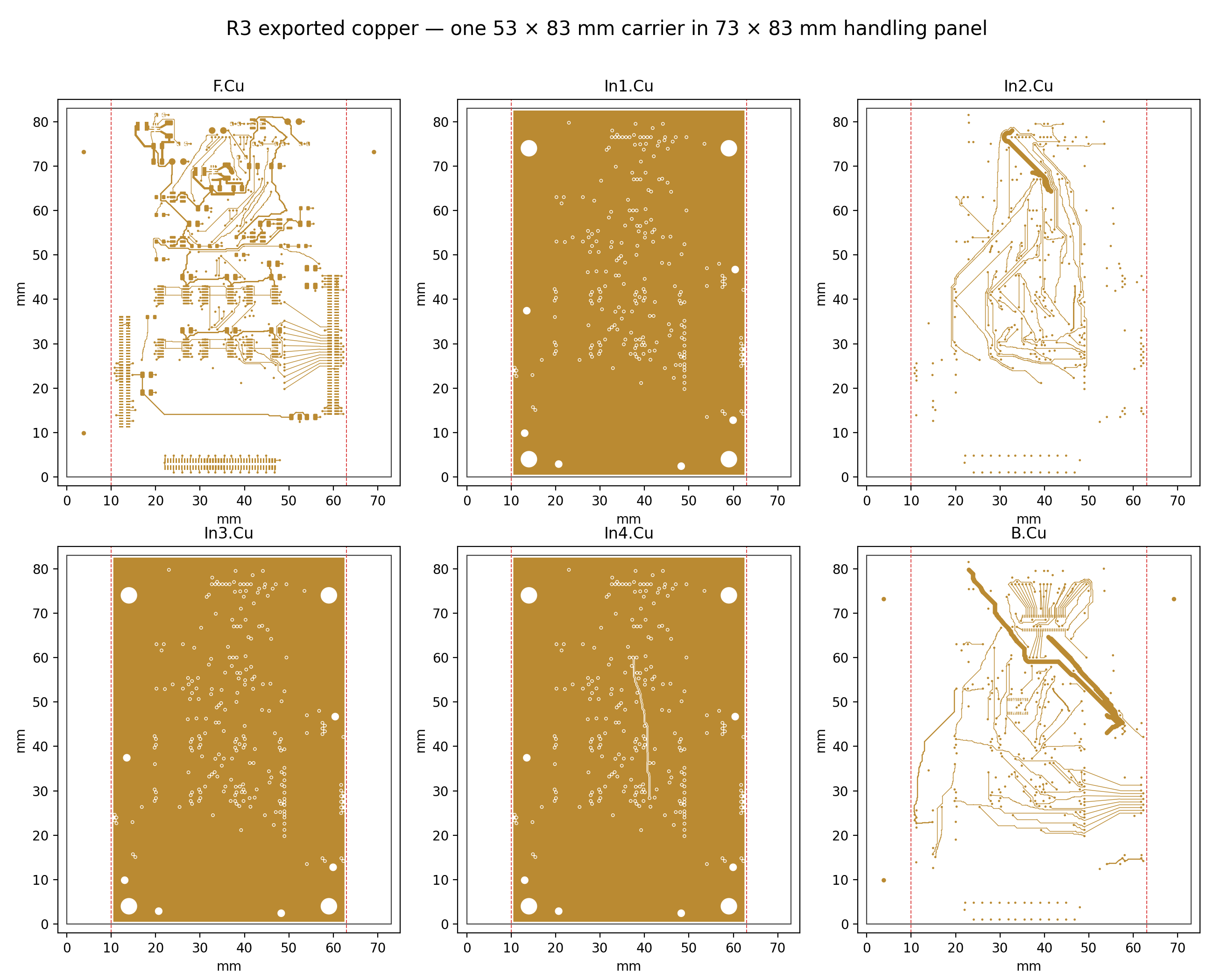
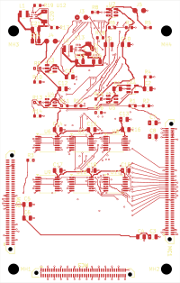
Native exports from the checked R3 board. View all six exported copper layers and handling rails.
Complete circuit
Open the complete PDF or use the embedded preview. The editable sheets are included in the KiCad ZIP. For readability, the PDF uses a documented print-layout copy; component and net topology are identical. Print-layout notes.
Manufacturing status
Native ERC, DRC, unrouted items and schematic/PCB parity are all zero. The Gerber/drill export passes 144 checks, and actual paste/mask/outline geometry passes 766 checks. No CAD checks are ignored or excluded.
JLCPCB must accept the fine connector/IC lands, filled vias, handling panel and soldering process. Exact component sourcing and placement orientation still need review. No factory approval or order has been obtained.
Six-layer FR-4, 1.6 mm, JLC06161H-3313 stack, 1 oz outer / 0.5 oz inner copper, green mask, white legend and ENIG. Specify epoxy-filled/capped all Ø0.30 mm vias. The two marked lines are V-cuts; remove the side rails after assembly. Follow the instructions inside the Gerber ZIP.
Check simultaneous connector seating, actual loads, startup and temperatures before attaching the ASIC. R5 ARM starts DNP/off. Aggregate VCCO commissioning is limited to 50 mA pending measured bank voltages. ASIC timing, firmware and powered operation remain unqualified.
Interface details
MC1 has 100 contacts; MC2 and MC3 each have 80. MC3 connects 28 ground contacts and reserves 52 explicit no-connects. J1 carries the mapped ASIC interface and named rails; J19 is a mechanical mating pair with its contacts explicitly NC. CLKH is supplied from FPGA to ASIC, while CLK32MHZ returns from ASIC to FPGA for capture.
J3 is the external 12 V input. J4/J5 are generated-rail test points. The existing LDO’s stimulation supplies and analog-ground contract remain separate. Signal-isolation and rail-supervision circuits are implemented in the R3 schematic; their actual assembled behavior still needs testing.
Preserved revisions
These earlier files retain their own revisions and checks. R3 publication does not approve fabrication, assembly or system operation.