Snapshot data could not be loaded. Do not rely on displayed counts; download the native project and reports below.
Smallest board ·
Loading current KiCad layout…
Front copper + fabrication labels · inner layers omittedDrag to pan · scroll to zoomBoth sides ↗
Routing evidence, dimensions and earlier studies
Working only on the smallest board. The 116 candidate digital ASIC nets and six ground-tie corrections are in the native design; AC_IN is separately reserved for an external analog source. Assignment is not completed copper. ASIC electrical limits, timing and hardware qualification remain open. Review uncertainties ↓
—signal nets have complete copper
—KiCad unconnected items remain
— / —track segments / through-vias
Size boundary. The current board remains 33 × 36 mm. J4 protrudes beyond the PCB edge; allow space for its plug and cable. Complete routing, assembly clearance, cable protection and thermal review may still require changes; no global minimum is claimed.
Snapshot identity and remaining copper
Native board SHA-256
Loading
KiCad version
—
Selected copper stack
— · JLC12161H1-1080B proposal; fabrication and impedance acceptance pending
Signal nets with no missing endpoints
—
Unconnected items by net
—
These are KiCad connectivity counts, not a percentage complete. Assigned power, pull-up and strap connections are routed. Routing must also meet return-path, impedance, power integrity and manufacturing requirements.
27 SEPTEMBER / CURRENT SMALLEST BOARD
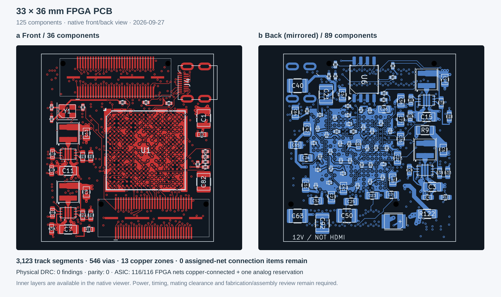
33 × 36 mm. Integrated rails and connectors.
The integrated board combines both mezzanines and the revised supply rails. The current audit records its component count, copper and any approved simplifications.
Current native board · click to zoom into layers, components and nets.
Complete the smallest version.
Configuration, flash, oscillator and JTAG now share 1.8 V. Bank 16 uses 2.5 V for the proposed LVDS transmitter. C92 supplies the separated bank 14 bulk allocation; R122 separates the converter sense node from distributed auxiliary capacitance.
Native KiCad: — physical violations; — unconnected items. The saved schematic and PCB are checked together. 116 mezzanine contacts have candidate FPGA balls; J5.46 is reserved for analog AC_IN. Three contacts remain reserved. Mating-board continuity, electrical limits and timing are unverified.
Layout space is working space: power paths, BGA escapes, ground returns and connector routes must fit around the parts. The inherited 0.010 mm minimum courtyard gap remains unqualified for assembly. J4 is aligned to the manufacturer edge datum; mating and plug-access checks remain open.
Earlier studies and the placement-only LaTeX report
Historical files remain available for traceability. Their copper counts, supply assignments and reports do not describe the current native board.
Five preserved design checkpoints.
Native design
Parts
Boot / bank 16
Unconnected items
What it establishes
Earlier core
126
3.3 V / 3.3 V
139
Earlier partial core; no ASIC connectors or application assignment
Rail revision
128
1.8 V / 2.5 V
347
C92/R122 and changed flash/oscillator; no mezzanines
Mezzanine fit
128
Inherited core placement
383
Both connectors fit in 2D; no integrated schematic or copper
Smaller placement
128
Inherited mezzanine study
383
37.5 × 36 mm; all study parts retained; no integrated schematic or copper
Earlier smaller placement · 26 Sep
128
Inherited 3.3 V core rails
383
33 × 36 mm; all 128 parts / 807 pad records retained; no integrated schematic or copper
The first three retain their 40 × 36 mm outlines. The earlier smaller placement is 37.5 × 36 mm; the later placement is 33 × 36 mm. Both remain separate placement studies; see the earlier native verification below. These historical unconnected counts covered assigned nets only and excluded the then-unmapped 117 application signals. They do not measure percentage complete. Download each separately.
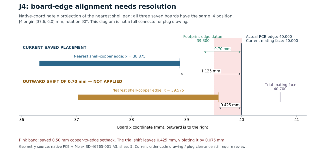
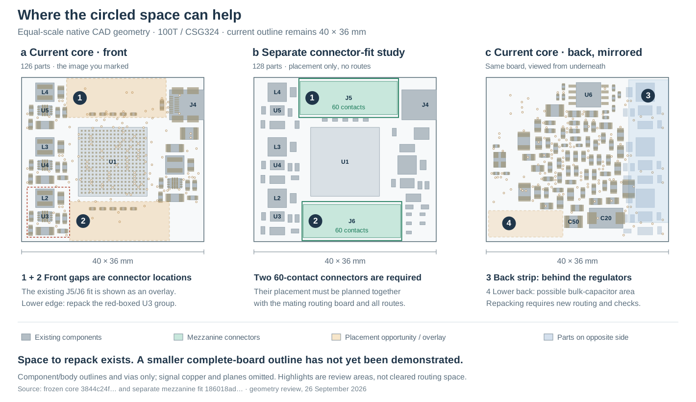
Connector fit needs correction. J4’s manufacturer board-edge marker is 0.70 mm inside the earlier core edge (0.10 mm in the smaller placement). Moving the port outward also conflicts with the present 0.50 mm copper-to-edge rule. Plug access, edge geometry and fabrication clearance must be resolved together. The smaller placement explicitly moves J4 and the outline; its saved clearance rules are retained.
See the connector-edge discrepancyMeasured coordinates from the three original 40 × 36 mm boards. The hypothetical shift illustrates the clearance conflict; it is not an approved correction.
SEPARATE PLACEMENT STUDY
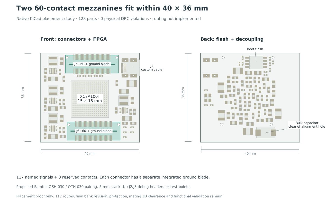
Two 60-pin mezzanines inside the same outline.
The 128-part candidate fits the connectors and revised 1206 input capacitors within 40 × 36 mm, with zero native physical DRC violations. It is intentionally unrouted: all tracks were removed and all 120 connector signal pads remain unassigned.
This is not the current core copper revision. The later C92/R122 bank-rail additions, cable damping/protection, mating-board 3D clearance and complete routing still need integration. Final size is not released.
Placement candidate only · click to enlarge. Nominal 5 mm pair: manufacturer fully mated spacing 5.03 mm; maximum separation adds 0.178 mm. Footprint offset discrepancy and mating orientation remain documented review items.
26 SEPTEMBER / SMALLER PLACEMENT + COMPLETE PIN REPORT
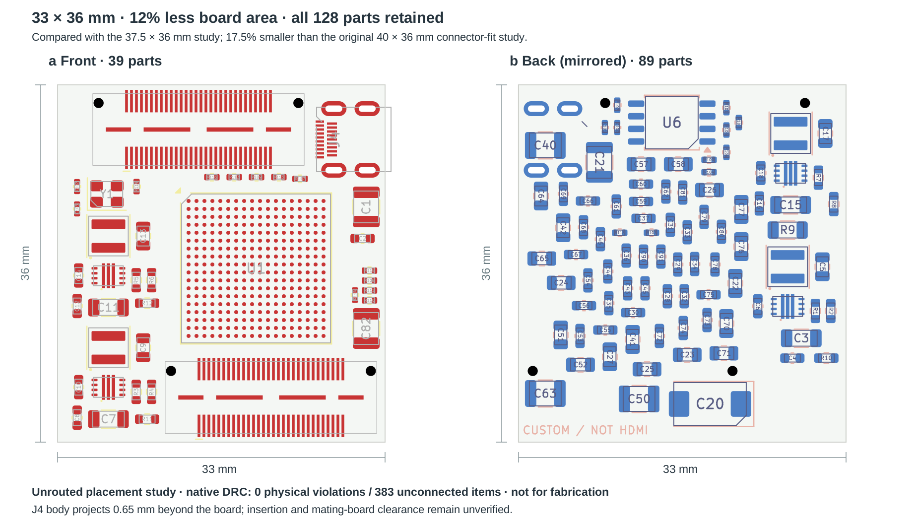
33 × 36 mm. All 128 study parts.
12% less area than 37.5 × 36 mm; 17.5% less than the original 40 × 36 mm connector-fit study. Both 60-contact mezzanines remain. Full wiring and qualification are unfinished.
39 front / 89 back · click to inspect native layers. 0 tracks, 0 vias and 0 zones.
Repack the available space.
J5 and J4 shift left. Two intact back-side regulator groups translate; the complete clock group rotates into the front upper-left area. Supporting capacitors and resistors fill smaller pockets. U1, J6 and the two front regulator groups stay fixed.
Empty space is still needed: courtyard boxes occupy approximately 80.6% of the front and 52.7% of the back. Remaining pockets must accommodate BGA escape, power distribution, returns and connector routing; these percentages do not establish route utilization.
Native KiCad DRC: 0 physical violations; 383 unconnected items. Fresh native readback preserves all 128 parts and 807 pad records. All 120 mezzanine signal contacts remain unassigned; the 117 ASIC signals still need FPGA assignment and routing.
The minimum courtyard gap is approximately 0.010 mm (0.009999 mm after coordinate rounding); assembly tolerance remains unqualified. J4’s drawn body overhangs the board by 0.65 mm, giving a 33.65 × 36 mm board-plus-body envelope. Plug insertion, mated-board clearance and full assembly dimensions remain unverified. Rail revision, protection, thermal and return-path work remain open. No global minimum or fabrication release is claimed.
What the original circled spaces containOriginal 40 × 36 mm geometries aligned by physical position; historical explanation, separate from the earlier 33 × 36 mm layout.
The placed-component inventory below is taken from the preserved 33 × 36 mm native board. It covers the headstage PCB only; the carrier, cable, power source and receiver are separate.
125placed parts per board
36distinct purchasing lines
1PCB, fabrication quote needed
Draft sourcing list · hold orders. Part numbers and quantities reproduce this 100T checkpoint, which is not released for manufacture. Check the chosen revision, electrical ratings, mating and assembly before ordering. Quantities exclude spares, build yield and supplier minimums. The newer 50T micro-HDMI proposal is a separate unrouted board with unresolved parts and a 5 V proposal that does not match its native 12 V net.
Fabricated 12-copper-layer PCB and assembly service; final stackup, assembly spacing and connector fit need review.
Two matching carrier-side connectors and the ASIC/routing assembly; exact mating height and contact map need confirmation.
Assembly quantities, spare allowance and supplier packaging must be calculated for the intended build count.
Needed to power and test it
A specified passive micro-HDMI cable and protected custom breakout or receiver. This connector carries a proposed power/JTAG/data assignment; do not attach ordinary HDMI equipment.
Regulated, current-limited bench source for the checkpoint's 12 V proposal and a 1.8 V-compatible target JTAG adapter. Source, cable current and entry protection remain unqualified.
Carrier-side analog AC_IN source, continuity and power test access. A full-rate receiver and PC capture path still need design and validation.
Source: native-board component inventory, board SHA-256 2975050c28c89fc96bf781cf082bffffc84189e6720ce05c4200d8552ac298fc. The 36 rows include all 83 capacitors, 28 resistors, 6 ICs, 4 inductors, 3 connectors and 1 oscillator placed on this board. Six schematic power flags are nonphysical and are excluded.
02 / COMPONENTS
Why is each part here?
The functions are necessary. The exact component population is not yet proven minimal.
Component evidence could not be verified. Use the dated audit below.
Loading components…
Choose a component to see its purpose and connections.
R12, R106, R107, R113 already removed. Further reductions require preserving each circuit function; capacitor removal needs power-integrity evidence.
The release target includes the entire chain. A bootable FPGA core alone does not satisfy it.
a
8 ASICs
88 output lines + 29 controls / clocks
116 FPGA + 1 analog contact
→
b
100T board
Capture · timing · control Packetization / link RTL
Core in progress
→
c
Custom cable
Data · power · JTAG Type-D connector
Contract being designed
→
d
XEM8310 → PC
Receiver · buffering USB / host recording
Integration unverified
What this board contains
XC7A100T CSG324: 324 balls, 210 user I/O, 0.8 mm BGA pitch. Selected order code: XC7A100T-1CSG324I; the operating load and thermal envelope remain unqualified.
Power: four TPS62135 converter circuits for core, auxiliary/configuration, 2.5 V link-bank and 1.5 V ASIC-facing I/O rails. Regulator input capacitors C3/C7/C11/C15 have been corrected to 22 µF, 25 V, 1206 parts after a DC-bias review. Rail assignments and physical power delivery still require qualification.
Smaller layout; assembly and bring-up must define access through the port or existing pads.
SW1, D1, R120
Manual reset and indicator removed. No assumption of a fitted status LED.
The retained flash supports independent cold boot; it has not been programmed or tested on this board. The XEM8310 is an FPGA module, not a conventional MCU. A receiver carrier/adapter and its firmware are still needed.
03 / PIN LABELS
116 FPGA signals. One analog contact.
Every ball and contact has a visible status. Select one for its name, bank and connection.
116 + 1candidate FPGA nets + analog reservation
3mezzanine contacts held in reserve
8cable data contacts awaiting assignment
Six pin definitions corrected: U1.L9/L10 and U2–U5.4 (FB2) are now assigned to GND. Their GND-net copper status is shown in the pin map and current audit. AC_IN is analog 0–1.5 V: J5.46 has no FPGA connection; U1.A13 is NC. IMP_TST is assumed digital 0/1.5 V; polarity remains open.
117 ASIC contacts, cable map and Gerald’s slide evidence
03 / INTERFACE CONTRACTS
117 contacts: 116 FPGA signals + analog AC_IN.
117 is the corrected logical signal budget. It does not include grounds, power, shielding or connector spare contacts.
ASIC interface: 117-contact baseline
Connector direction: two 60-pin mezzanines. Samtec QSH-030-01-L-D-A / QTH-030-01-L-D-A with a 5 mm mated stack is a proposed implementation; footprint, mating orientation and contact map are still under review. Dedicated ground blades are separate from the 120 signal contacts.
4× L/R for stimulation chips; 2× L/R for non-stimulation boards
ASIC outputs
88
8 ASICs × 11 output lines
SPI clocks
4
Four additional SPI_CLK lines
Total
117
Corrected September 24 baseline
The earlier interface deck expands 11 outputs into 8 DATA + returned CLK32MHz + READ + SYNC: 64 data and 24 timing/control outputs. Preserve that distinction when specifying timing.
Five user I/O serve SPI x1 flash, the oscillator and PUDC_B. The 116 candidate FPGA signals use banks 15, 34 and 35, leaving 34 positions in those 1.5 V banks and 81 intentionally unused FPGA balls plus eight future-link reservations overall. AC_IN is now an external analog reservation, not GPIO. All eight returned clocks have positive clock-capable balls; actual capture placement and timing remain unverified. Four complete bank-16 pairs fit the proposed cable lanes; its other two pins are not a fifth pair.
J4: custom powered Type-D link
Contact
Current board net
Role
1
VCCAUX_1V8
Target-voltage reference
2 / 15 / 17 / 18
TMS / TDI / TCK / TDO
Dedicated target JTAG
19
LINK_12V
Proposed nominal 12 V input
16
GND
DC return
4 / 7 / 10 / 13 / shell
GND
Pair shields / connector shell
3/5 · 6/8 · 9/11 · 12/14
Unassigned
Four reserved data pairs
Custom electrical interface. Do not connect ordinary HDMI equipment. Contact numbers are physical Type-D contacts; cable continuity, orientation, return current and hot-plug protection need verification.
The XEM8310 receiver assembly will supply the custom cable through a designed carrier/adapter. The proposed carrier branch is 12 V ±5%, with a 0.60 A continuous load limit and a maximum 0.30 m custom cable. Voltage drop, fault protection and hot-plug behavior still require qualification. This does not assert that an unmodified XEM8310 can directly power this board.
The development proposal uses three LVDS data pairs plus one forwarded clock, with 12-bit packed samples. Exact XEM8310 contacts, timing closure, common-mode handling, receiver bias/termination and the target-JTAG bridge still require implementation and verification. Direct DC coupling has no guaranteed allowance for positive cable ground offset at the published transmitter/receiver limits. The module’s own JTAG does not automatically program this target. The current board requires a verified 1.8 V target-JTAG interface. BOARD_READY is an initialization signal, not a continuous rail monitor. Read the source-backed development architecture.
GERALD’S ORIGINAL ASIC SLIDES
More of the protocol is known.
Slides 14–17 identify each ASIC’s eight data outputs, returned clock, READ and SYNC. They show 1,024 clocks per frame and 16 READ groups. Each group has 16 zero clocks followed by 48 clocks carrying four interleaved 12-bit samples.
Slides 25–28 describe FPGA-to-ASIC SPI CLK, L, R and LATCH, then configuration → STIM_EN → STIM_START → charge balancing after 64 STIM_CLK cycles. L and R are both configuration data outputs.
Two conflicts need clarification.
Stimulation timing: slide 18 says 64 clocks = 2 ms, GUI examples use 32 µs per step, and slides 27–28 label 60 kHz. These are not one agreed timing requirement.
Channel labels: the table in slides 15–17 repeats channels 57 and 49 and omits 50 and 59. We retain the original source and flag the apparent errors; a corrected chip map still needs confirmation.
The slides establish useful behavior. Gerald’s later answer specifies nominal 1.5 V, analog AC_IN, falling-edge sampling and SPI → digital/analog resets → recording clock. The chosen interpretation uses eight returned clocks and four outgoing board clocks; timing margins and startup waveforms remain open. Latest answers and assumptions ↗
A clean geometry check cannot establish correct circuitry or working hardware.
—physical rule violations
—gaps on assigned nets
—intentionally unused pins
The 116 candidate GPIO assignments, external analog reservation and six GND ties are in CAD. 83 pins are intentionally unused and labeled NC. Separately, 19 endpoints reserve future interfaces: eight FPGA balls, eight cable contacts and three mezzanine contacts. Missing copper is counted separately. The current routing audit supplies the measured results.
Read the measured checks and their limits
04 / EVIDENCE
What has actually been checked.
Checks below describe the downloadable snapshot. No result is a substitute for the missing full-board interfaces or a powered bench test.
Check
Observed result
What it establishes / limit
Native project and netlist
— endpoints match
Exported schematic endpoints correspond to PCB pads. — schematic pages and local libraries included.
Native KiCad DRC
— geometry violations — schematic parity issues
Saved rule checks pass for routed geometry. — ignored checks and — exclusions. Connectivity and engineering qualification remain separate.
Copper connectivity
— unconnected items
— signal nets have complete copper. Unconnected counts cover assigned nets, including the 116 candidate ASIC GPIO nets, and exclude unassigned endpoints. Electrical timing, power delivery and hardware operation remain unverified.
Schematic ERC
— open pins + — other errors + — warnings
83 unused pins are explicitly NC-marked. The 19 reserved endpoints remain visible, as do four FB2/GND electrical-model conflicts and the single-pad analog reservation warning. Read the current audit; these counts do not establish a completed schematic.
116 FPGA + 1 analog contact
116 assigned / — copper-connected
Candidate digital signals have connector contacts and FPGA balls. Analog AC_IN has a separate contact with no FPGA path. These assignments are provisional; completed copper, ASIC electrical compatibility, mating continuity and capture timing require separate verification.
RTL / timing / data link
Raw capture simulated
Four full-depth synthetic capture cycles pass across eight independent clock domains. XC7 synthesis passes. Vivado timing, startup, JTAG readout and the receiver remain unfinished.
Smallest-board integration
Native readback and parity
C92/R122 and the revised boot parts are included. The current audit records component changes and verifies the native population and pad assignments. Earlier independent audits are retained in the history section.
Power / signal integrity / DFM
Qualification pending
Workload currents, rail transients, cable current, signal/return-path analysis, thermal margin and fabrication/assembly acceptance remain required. The stackup and exact BOM parts are selected.
Built hardware
Not tested
No measured power-up, JTAG identification, cold boot or data capture from this design.
Detailed uncertainty register and release criteria
Current update: U1.L9/L10 and U2–U5.FB2 are assigned to GND; the current audit reports copper continuity. The 116 candidate digital nets are provisionally assigned; AC_IN is an external analog reservation. Earlier evidence in this register remains historical.
05 / COMPLETION CRITERIA
Uncertainties and the work ahead.
Each item states what is known, what is still uncertain, who should resolve it and what evidence will close it. Owner roles are proposed, not accepted assignments.
Six remaining work areas
Only the first item needs an ASIC-team specification. The other items are implementation and verification work; owner roles are proposed.
Showing 6 of 6 uncertainties.
ASIC specification and mating boardTeam information
Established: Gerald confirmed nominal 1.5 V, analog AC_IN and falling-edge capture. The selected interpretation uses eight returned clocks and four outgoing board clocks.
To finish: Confirm the physical chip/contact map, digital pad limits, input loading and unpowered behavior. Provide guaranteed clock/data delays, SPI values and reset polarity/pulse widths. IMP_TST is provisionally digital; its inactive state remains open.
Owner: Gerald / ASIC and routing-board designers; FPGA integration checks the supplied specification.
Firmware and timing proofEngineering work
Established: Master SPI x1 boot removes two optional quad-data links. Finite raw-capture logic passes synthetic-data simulation and XC7 synthesis. A separate package/clock proof design is supplied.
To finish: Implement the real SPI → resets → clock startup, JTAG readout and revision-specific top level. Run Vivado placement, clock-resource, CDC and timing checks with real ASIC delays. No programmable bitstream is supplied.
Owner: FPGA firmware / Jiaao, using the ASIC specification. Earlier ECP5 code provides a baseline; its returned-clock startup dependency and uninitialized SPI-default path need correction.
Power margins and custom input cableEngineering work
Established: The four-rail circuit, bypass parts and 12 mΩ core isolation part are selected. Current routing status is measured separately above.
To finish: Verify workload currents, capacitor bias, shared mounting-via paths, rail transients and heat. Build the controlled-rise, current-limited 12 V source and verify the actual cable. The source protection is not fitted to this FPGA board; the XEM8310 does not automatically provide 12 V output.
Owner: FPGA power design and source/carrier design. The 2 A / 85 °C calculation is a screening case, not a guaranteed rating.
Assembly, stackup and connector fitEngineering work
Established: XC7A100T-1CSG324I and the Molex 467651001 port are selected. The physical proposal is JLC12161H1-1080B, 12 layers. The board outline remains 33 × 36 mm.
To finish: Obtain fabrication/assembly acceptance of the connector slot tolerances, small-part clearances and BGA process. Check both mezzanine mating footprints, stack height, pin-1 orientation and plug access. Verify impedance and return paths on the final routes.
Owner: PCB/mechanical design and fabricator/assembler review. No order is authorized or placed.
Full XEM8310 acquisition linkEngineering work
Established: Eight FPGA balls and eight cable contacts reserve four differential pairs. They are visibly labeled R; the receiver module is an FPGA/USB module.
To finish: Complete the carrier contact map, compatible voltages, receiver network, target-JTAG bridge, packet format and host-stall handling. Route the chosen link only after its electrical contract is established. This remains part of the full system, beyond the first finite capture.
Owner: FPGA / XEM8310 carrier and acquisition-software design.
Measured operationBench measurements
Established: CAD checks and simulation are available. No assembled board has demonstrated operation.
To finish: After design release and assembly, check rails and current, JTAG ID, configuration recovery and clocks. Capture a known pattern, then one ASIC and all eight; measure thermal and sustained acquisition margins.
Owner: Lab integration, using a revision-specific test procedure.
Requirements for manufacturing and hardware acceptance
Interface closure Open
Validate the proposed two 60-pin mezzanine footprints, mating stack and contact map, including ground blades and any power contacts; approve the provisional FPGA balls, bank voltages, clock inputs, timing and startup behavior. ASIC / routing handoff: Howard, Zitong and Gerald.
Receiver and powered cable Being designed
Implement the XEM8310 carrier/adapter, source current and protection, cable continuity/length contract, data protocol, termination and target-JTAG access. Verify throughput and current margins with the actual cable.
Assigned copper review Connected · review open
The native audit finds 116/116 assigned ASIC digital nets connected and 0 assigned-net gaps. Review supply mounting paths, reference-plane continuity and signal timing. The later cable data interface still needs its electrical contract and routing. Copper continuity does not establish powered operation.
Manufacturing review Not passed
Review the selected exact parts, physical stackup and fabrication rules; close native ERC/DRC and netlist checks with reviewed exceptions; complete Vivado pin/timing, SI/PI, thermal and assembler DFM review. Only then export and independently inspect Gerbers, drills, BOM and placement files.
Hardware acceptance Not started
Bring up current-limited power and rails, read JTAG ID, program and cold-boot flash, check clocks and all ASIC channels, then verify sustained XEM8310 → PC → disk recording with error counters and a reproducible test record.
Earlier project archives and the placement-only LaTeX report
The 31-page report describes the earlier 128-component, unrouted placement. The learning PDF explains the previous 130-component snapshot; use the current routing audit for today’s assignments and copper.
These are review files, not fabrication outputs. No manufacturing package is released. Source views and reports are frozen to the board hash shown above; earlier audits retain their own dates and are not silently presented as current copper verification.
Design references and earlier decisions
AMD UG470 — 7-series startup, SPI configuration and JTAG.