CURRENT WORK · R12
One 19-contact link first.
The single-link schematic is implemented. The current native layout is in progress; ground and JTAG routes remain open.
PRESERVED THREE-PORT ARCHITECTURE · R10 STUDY
Three custom FPGA boards into one XEM8310.
Circuit map · R10 HDI studyEach custom XC7A25T board has its own 19-contact µHDMI cable. A proposed interposer sits at the MC1/MC2/MC3 joint between the purchased XEM8310 and BRK8310, and gives each cable one four-channel GTY bank. XEM USB is the initial path to the PC. The three-port circuit is mapped; the physical adapter and complete link are still being designed.
3 custom FPGA boards3 cables and receptacles3 XEM GTY banks1 XEM + BRK stack
NATIVE KICAD SCHEMATIC · EIGHT SHEETS
Inspect the actual connector circuit.
Three-port adapter circuit mapOverview · one sheet per cable · power/GPIO · MC1/MC2 pass-throughs
Open large schematic viewer ↗Choose a sheet, zoom, then drag to inspect the pin labels. This is the preserved logical schematic carried from R8 into the routing studies; protected 12 V branches and JTAG headers remain circuit placeholders. Open the complete schematic PDF ↗ · View the separate custom FPGA schematic ↗
ASSEMBLY VIEW
See each board separately, then see how they connect.
Exploded hardware viewXEM8310 above · proposed interposer at MC3 · BRK8310 below · three FPGA boards remote
Open 3D view ↗The XEM8310 and BRK8310 models are from Opal Kelly’s PCB-derived STEP downloads when shown in the viewer. The current 25T placement is exported from native KiCad; its PCB is unrouted and the DF40 connector interface is under redesign. The default interposer mesh is native R9, with six routed GTY pairs. The revision buttons also offer R10, with all twelve selected pairs traced through a proposed HDI process, and preserved R8. R10 still has 97 open items and no qualified impedance, reference planes or pair matching. Its small blind vias need a selected fabricator and stackup. The view explains architecture; it is not a fit certificate or a fabricated assembly.
OPTIONAL R10 PCB · HDI ROUTING FEASIBILITY
All twelve signal pairs now have a copper path.
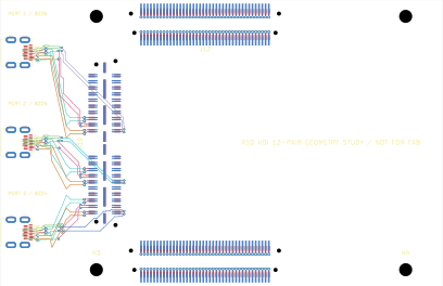
MANUFACTURING STUDY · PROCESS NOT SELECTED
Small blind vias solve the inner-contact escape.
R10 connects TX0, TX1, reserved TX2 and control for all three cables using twelve proposed 0.25/0.10 mm laser microvias. The independent audit confirms all 24 signal contacts and 160 MC1/MC2 paths. Physical DRC is clear under the documented HDI trial rules, but 97 items remain open. Power, JTAG, returns, impedance and pair matching are unfinished. A fabricator must qualify the via process and stackup before this route can be selected.
Inspect R10 in 3D ↗Download R10 KiCad project ↓Read exact rules and remaining work ↗This is a connected-endpoint geometry study. Individually routed tracks are not yet a controlled-impedance, coupled differential channel. R9 remains the default 3D baseline; select “R10 · 12 pairs · HDI study” to see this optional native revision. Both earlier studies remain preserved.
NATIVE R9 PCB · SIX-PAIR ROUTING STUDY
Compare the preserved six-pair route.
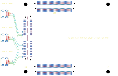
PARTIAL BOARD FILE · OPEN IN KICAD
Six routed pairs, no complete cable link yet.
R9 traces TX0 and reserved TX2 on each of three cables and preserves all 160 MC1/MC2 pass-throughs. TX1 and the reverse control pair are open on every cable. KiCad reports zero physical violations at the provisional 0.15 mm study rule, 109 unconnected items, and 19 schematic-parity warnings. Power and JTAG hardware are still schematic placeholders. The first full-route attempt failed because ordinary through-vias collided with the Type-D connector keepout and other copper; its DRC record is preserved in the local R9 study.
Download R9 KiCad project ↓Read route limits and validation ↗The six-pair route is a geometric study only. Its copper has no verified impedance, length matching, reference planes, cable loss, or complete data/control path. The 3D view uses the native R9 PCB export by default and offers the earlier R8 board as a separate selection; board fit and cable approach remain unverified.
EARLIER R8 PCB · ONE-PAIR SAMPLE
Compare the preserved first PCB study.
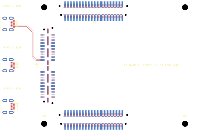
BOARD FILE · OPEN IN KICAD
Three receptacles, one routed data pair.
R8 has 160 MC1/MC2 pass-through contacts routed and one MC3-to-Type-D pair as a routing sample. Another 119 items remain unconnected. The conservative 0.20 mm DRC reports 61 physical findings, and JTAG/power circuits are still schematic placeholders.
Download editable KiCad project ↓Read board status and source notes ↗Select R8 in the 3D receiver view to load this earlier native PCB shape. Its stack connector bodies are absent from the KiCad export; the manufacturer's XEM/BRK models show their own connector geometry. Board placement, cable approach and vertical separation remain unverified.
SIGNAL ROUTE
One cable gets one GTY bank.
01 · EXISTING MODULEXEM8310MC3 GTY RX receives recordings; TX0 returns control
USB → PC
USB → PC
02 · NEW BOARD PROPOSALThree-port interposerJ201/J202/J203 · route to XEM MC3
selected BRK GTY contacts isolated
selected BRK GTY contacts isolated
03 · EXISTING BREAKOUTBRK831012 V input arrangement · J6 PCIe alternate future mode
Directions are relative to each custom FPGA: its recording TX pairs enter XEM RX pairs; XEM TX0 sends framed control back. The third recording pair is physically assigned but reserved in the current two-lane 25T plan. The three links are intended to operate together. In that mode BRK J6 cannot also use its x8 GTY paths.
R7 EXACT CONTACT ALLOCATION
Three identical cables, three different MC3 banks.
| Cable / FPGA board | Recording 3/5 → RX0 | Recording 6/8 → RX1 | Reserved 9/11 → RX2 | Control 12/14 ← TX0 |
|---|---|---|---|---|
| J201 · FPGA A Bank 226 | MC3 41/43 | MC3 45/47 | MC3 49/51 | MC3 42/44 |
| J202 · FPGA B Bank 225 | MC3 21/23 | MC3 25/27 | MC3 29/31 | MC3 22/24 |
| J203 · FPGA C Bank 224 | MC3 1/3 | MC3 5/7 | MC3 9/11 | MC3 2/4 |
Every 19-contact cable
1 is the custom FPGA’s 1.8 V JTAG voltage reference (sense only). 2 TMS, 15 TDI, 17 TCK and 18 TDO serve its JTAG target. 4/7/10/13/16 are grounds. 19 is assigned 12 V in the proposed custom cable; the protection circuit is still unbuilt. Shield bonding is unresolved.
At the XEM / BRK joint
The selected eight conductors per bank go to the cable only; matching BRK contacts are open to avoid high-speed stubs. R9 and R10 preserve physical routes across all 80 MC1 plus all 80 MC2 contacts. MC2 1–4 and 5–8 are VDCIN and DGND respectively, but their traces and current capacity remain unqualified. R10 connects all twelve selected signal pairs; power/JTAG branches, returns and other board connections remain unfinished.
This table follows the Opal Kelly XEM8310 pin list and the R7 five-page KiCad schematic. A GTY channel includes independent receive and transmit halves, so the candidate uses channel 0 RX for recording and channel 0 TX for control. GTY clocking, lane alignment and simultaneous transfer are not yet demonstrated.
THREE DISTINCT BOARDS IN THE RECEIVER STACK
Where to look on the hardware in the lab.
XEM8310
FPGA module with USB and twelve full-duplex GTY channels. Its underside vertical MC3 connector is the high-speed contact set used here; MC1 and MC2 are separate mates.
XEM expansion connector guide ↗Three-port interposer
A new PCB would mate between the existing boards, break three MC3 quads out to three µHDMI receptacles, route input power to protected branches and preserve chosen lower breakout functions. The latest R10 HDI study has three receptacles, six stack-connector footprints, four holes and twelve selected signal pairs traced; it still has 97 open items and no approved fabrication process. Power protection and JTAG probe headers are schematic placeholders, not placed hardware.
Inspect proposed position ↗BRK8310
The lab’s breakout carrier currently mates directly to XEM. Its J1 Bulls Eye serves bank 226 and J6 is the PCIe card edge for banks 224/225. J6 is unavailable during three-cable acquisition.
See XEM + BRK detail ↗ENGINEERING STATUS
What this drawing proves, and what remains to check.
Mapped in the KiCad R7 schematic
Three 19-contact ports, MC3 bank 226/225/224 pins, separate JTAG probe paths, isolated matching BRK GTY contacts and MC2 input-power contacts. The logical netlist and ERC checks passed. R10 physically connects all 160 MC1/MC2 paths and all twelve selected GTY pairs. Its independent contact audit passed. Branch-power/JTAG circuits, returns and other board connections remain incomplete.
Needs PCB and assembly verification
Actual mating footprints, orientation, stack height, fansink/bracket clearance, impedance and loss, GTY impedance and pair geometry, return paths, 12 V protection and load budget, shield/ESD, and Vivado GTY link proof. R10 has 97 unconnected items and 19 schematic-parity findings. Its physical DRC is clear under provisional HDI rules; this does not qualify the manufacturing process or establish a complete link. R9 and R8 remain separate.
USB capture still needs a rate test
Three boards stream at once, but the aggregate channel count is still to be confirmed. The actual total sample payload plus framing must fit sustained XEM USB, host and storage performance with an overflow policy.
PCIe is an alternate configuration
The J6 card edge shares GTY banks 224/225 used by two cables here. Keeping the possibility of PCIe later means a different population or adapter mode, not simultaneous PCIe operation in this layout.
The custom µHDMI cable assigns 12 V to contact 19, which is a nonstandard use of an HDMI connector. Do not mate it with ordinary HDMI equipment. Each of the three branches needs an explicit protected source, cable/contact current qualification and a power budget for its entire FPGA, routing and ASIC assembly.
REVIEW FILES AND MANUFACTURER SOURCES
Open the schematic and mechanical references.
Browsable eight-sheet circuit ↗R10 HDI study KiCad ZIP ↓R7 three-port schematic PDF ↗R7 complete KiCad project ↓R9 six-pair PCB KiCad ZIP ↓R9 eight-page logical schematic PDF ↗R8 partial PCB KiCad ZIP ↓R8 eight-page schematic PDF ↗XEM8310 official STEP ↓BRK8310 official STEP ↓XEM8310 pin list ↗BRK8310 guide ↗
The manufacturer supplies separate PCB-derived solid models for XEM and BRK. The interposer and cable positions in the assembly view are design representations and do not establish physical fit. Earlier one-port R3/R4 and direct-carrier R2 studies remain preserved; start with the R4 dated adapter history.