FPGA hardware · Weekly update

Weekly update

October 28, 2026

XEM8310 breakout board

Eight FPGA links and the current breakout design.

For discussion: How should we use the HDMI port?

XEM8305 / LDO carrier

Completed routing, with schematic, layout and 3D views.

Whole system assembly

Open full view ↗

ASIC stacks, LDOs and Artix-7 FPGAs connected through XEM8310/BRK to the PC

Thinner ASIC stack is a concept for review. Breakout routing and mechanical fit remain open.

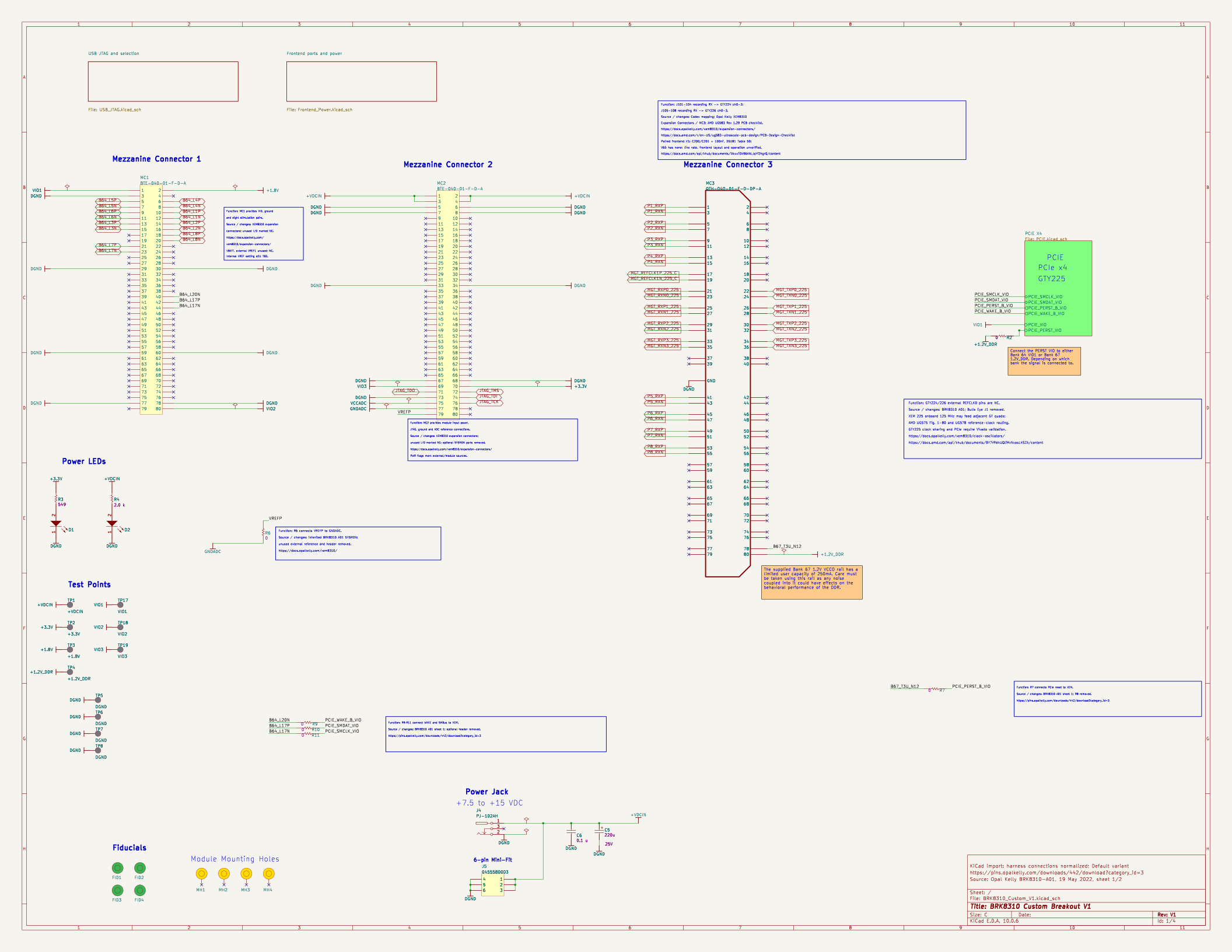
Breakout schematic and layout

BRK8310-derived XEM8310 design · 27 October working snapshot
Open PDF ↗
Breakout V1 schematic sheet 1
Layers, planes, parts and netsOpen full view ↗
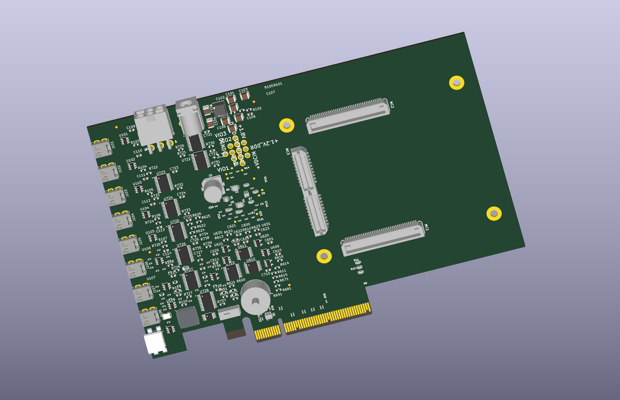
Initial breakout 3D view with provisional component placement

Work in progress: initial placement, unrouted. Connector fit and electrical checks remain open.

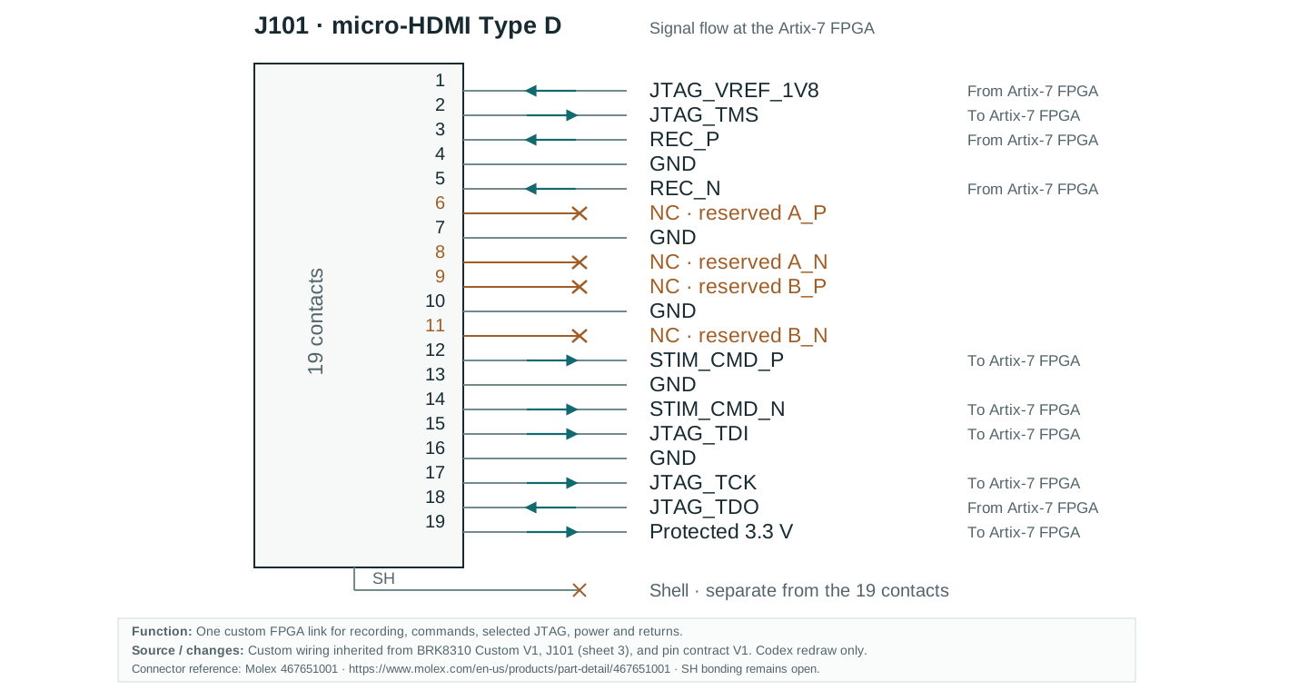
How should we use the HDMI port?
Open schematic ↗
Micro-HDMI nineteen-contact schematic. Pins 6, 8, 9 and 11 are unconnected reserved contacts. Shell SH is separate.

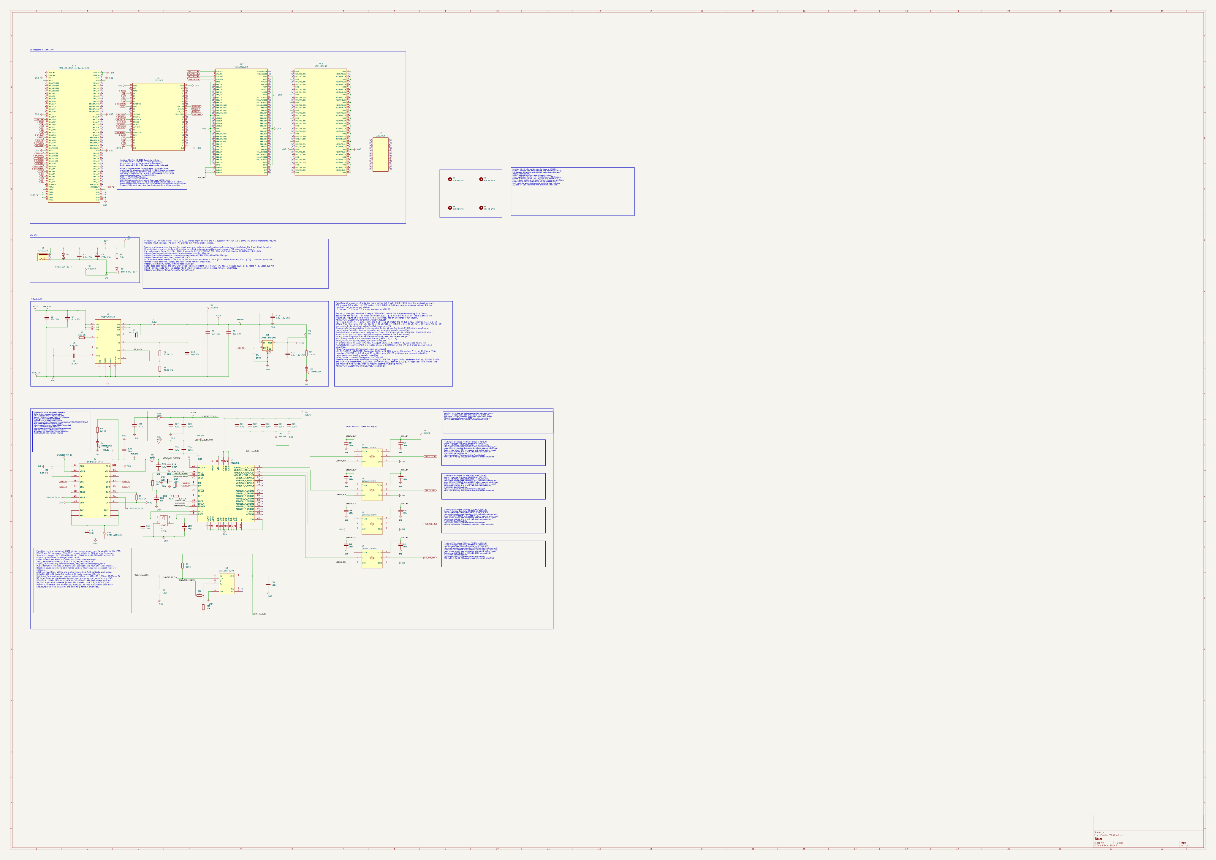
XEM8305 carrier for the LDO board

Latest schematic, routed board and 3D views
Open drawing ↗
Carrier schematic
Layers, planes, parts and netsOpen full view ↗
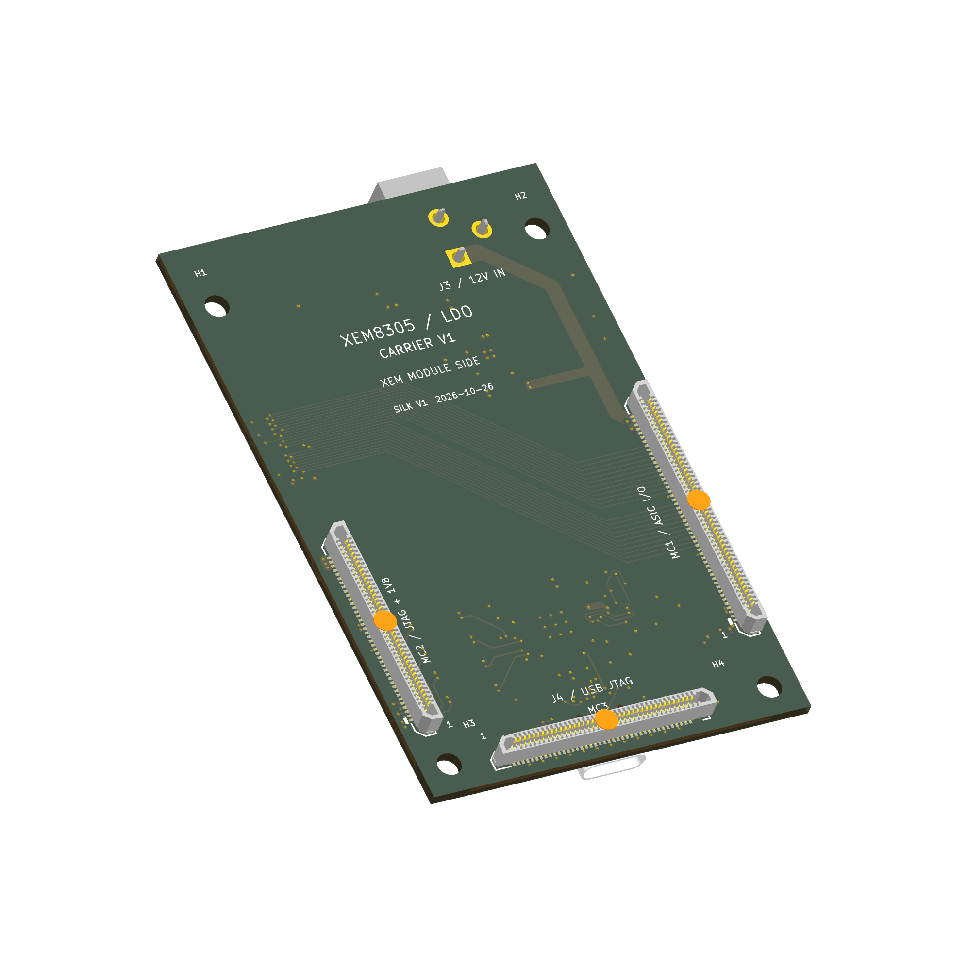
3D render of the latest carrier
Interactive assembly uses the 26 October model, before later copper edits.

Routing and native connectivity checks complete. Fabrication and powered testing remain open.

Next steps

  1. Settle the HDMI pinout, signals and cable requirements
  2. Continue the breakout design and placement review
  3. Update the Artix-7 FPGA interface as the HDMI decisions are confirmed

Later: thinner ASIC PCBs and lower-profile connectors

Comments

Shared on this presentation.

0 / 2000

All comments