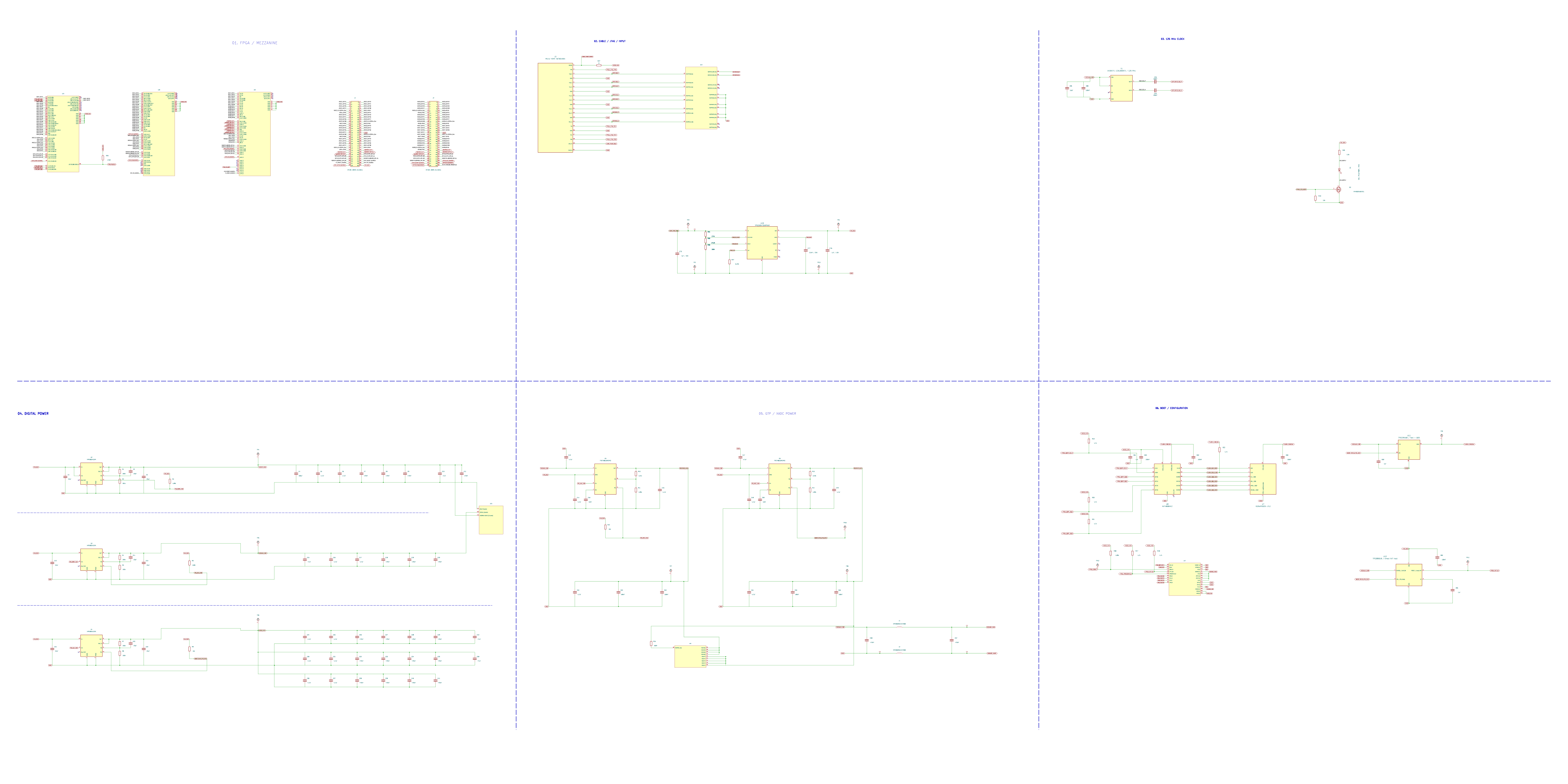
Carrier
Quick email review with Gerald, Zitong and JLCPCB; revised a few issues.
FPGA schematic
Power, pinout, clock and configuration on one page.
FPGA routing
116/116 digital mezzanine paths connected.
Carrier board schematic
- Power12 V powers XEM8305; an onboard buck provides 3.3 V to the LDO board.
- PinoutEight data lines plus clocks, SPI, reset and stimulation control at 1.8 V.
- ProgrammingUSB-C JTAG bridge with 1.8 V level translation. USB powers the bridge only.
- ConnectorsMC1/MC2 connect XEM8305; the 50-pin J1 links the LDO board.
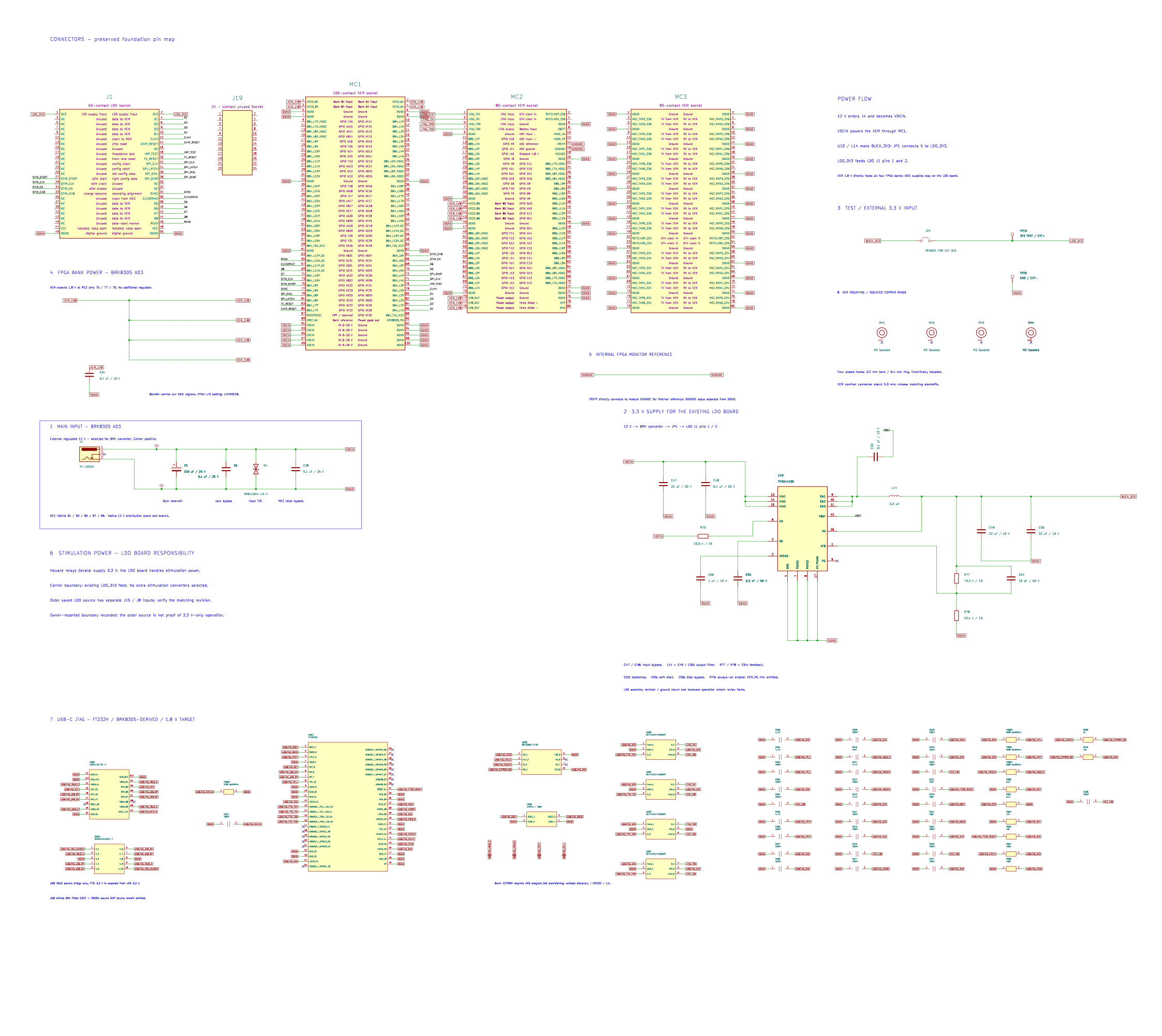
FPGA PCB schematic
- Power3.3 V input; onboard 1.0 V core, 1.8 V auxiliary and 1.5 V I/O rails.
- PinoutJ1/J2: two 60-pin connectors for eight ASICs’ data, clocks, SPI and control.
- Clock125 MHz differential reference to GTP REFCLK0; also used by FPGA logic.
- ConfigurationFlash stores the FPGA image; direct JTAG supports programming and debug.