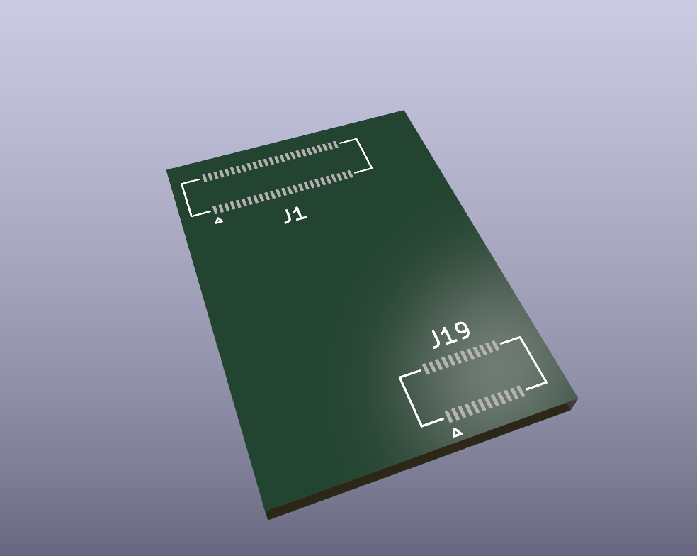
C2 small-board preview
18 × 25 mm provisional outline around the LDO connector centres. This dated mechanical study has unassigned cable connectors, components and tracks.
ONE-CHIP BACKUP · XEM BY CABLE
A small board on the existing LDO board. The XEM stays separate and connects through a cable.
WEEKEND UPDATE · 3–4 OCTOBER 2026
I finished routing the LDO adapter and added ground copper and stitching vias. Following Gerald’s suggestion, I added a separate locking VDD/GND connector, while keeping power off the signal flex cable. Both J1 and J19 are included mechanically, with J19 intentionally unconnected. The latest layout passes DRC and connectivity checks, and I’ve prepared a concise schematic and pin-to-pin guide. Before fabrication, I still need to verify the actual current requirement, analog-ground return, and cable/connector fit.
Published C2 mechanical preview · 2 October 2026. Size reference: the shared SpikeGadgets Rev. 2.5 board. Its photos have no verified dimensions; 18 × 25 mm is a proposed socket envelope, not a measured SpikeGadgets size.
Loading 3D concept…

18 × 25 mm provisional outline around the LDO connector centres. This dated mechanical study has unassigned cable connectors, components and tracks.
18.300 × 42.025 mm source envelope. J1/J19 face the routing board; J2 remains at the ASIC end.
The cable in this October 2 illustration is a functional path. The weekend update above records the later signal mapping and separate power connector.
J1 carries 23 ASIC signals, two 3V3 contacts and two DGND contacts in the supplied LDO CAD. Its VCC contacts 47/48 are isolated in that source. J19 is a PCB-only, netless footprint in the source; the latest adapter includes it mechanically and intentionally leaves it unconnected. Cable/connector fit still needs checking.
The source LDO outline and J1/J19/J2 centres come from the audited October 2 Gerald native PCB. The two LDO connector centres are registered to the new concept by a 180° face reversal and translation. This illustrates the board relationship; it does not prove connector mating, pin continuity, stack height or clearance.
The interactive view loads native KiCad PCB meshes: the separate C2 mechanical study and the existing Gerald LDO source. Available LDO component models and source copper are included; missing connector bodies remain omitted. The cable and XEM hardware are illustrative or omitted. The C2 study has no net assignments or tracks. The dashed cable endpoint is not a selected physical footprint. The exploded gap is illustrative.
C1/R4 direct-mate studies are historical and unselected. The October 2 instruction was a small board referenced to SpikeGadgets, with XEM connected by cable.
Native C2 mechanical checks are recorded in the review notes. This dated C2 preview has no electrical netlist, cable contact mapping or routing-completion claim; ERC does not apply to this mechanical-only study. Exact SpikeGadgets width × height and the selected cable with its endpoint pinout remain necessary design inputs.
Native small-board image ↗ · Source facts and registration ↗ · Review notes ↗ · Dated meeting context ↗